


348
340
平芯微PW1555A中文规格书
2024-04-19 13:41:11
0点赞
0收藏
0评论
一般描述 (百度翻译)
PW1555A 是一款可编程限流开关,具有输入电压范围选择和输出电压箝位功能。集成保护 N 沟
道 FET 的极低 RDS(ON) 有助于降低正常工作期间的功率损耗。可编程软启动时间控制启动期
间输出电压的压摆率。独立的使能控制允许复杂的系统排序控制。它集成了过温保护、关断和自动
恢复与迟滞功能。
该 IC 采用小尺寸 DFN3X3-10,可提供小 PCB 面积应用。PW1555A 为可选三段电压设置, 3.3V, 5V, 12V,不是连续电压,连续输入电压如 PW1558 和 PW1605 。
特点
⚫ 宽输入电压范围: 2.5V 至 14V,浪涌高达 30V
⚫ 极低的 RDS(ON) 用于集成
⚫ 保护开关: 40 mΩ
⚫ 可编程软启动时间
⚫ 可编程电流限制
⚫ 短路保护
⚫ 可选输入范围和箝位输出电压门限
⚫ 使能接口引脚
⚫ 热关断保护和自动恢复
⚫ 符合 RoHS 标准且无卤素
⚫ 紧凑型封装: DFN3X3-10
应用
⚫ 服务器
⚫ 服务电脑
⚫ 笔记本电脑
⚫ 垫迷你
典型应用电路
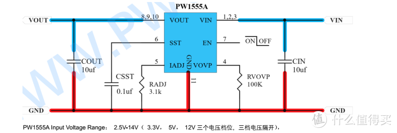
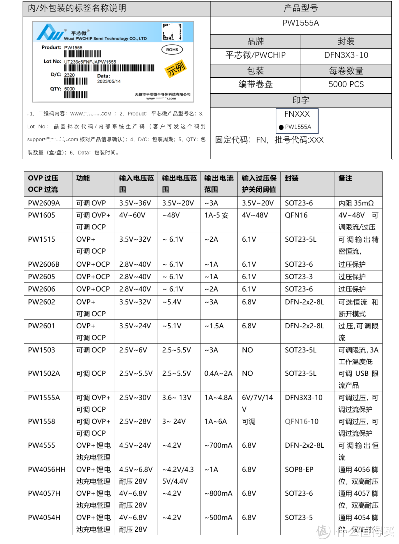
同类型产品 PW1558 限流+过压 ( 3V~ 20V 5.8A); PW1605 ( 4V~ 48V 5A); PW1503
(2.5V~6V 3A); PW1515 (3.5V~6V 2A) ,单独过压产品: PW2609A(3V~ 20V 3A)
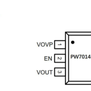
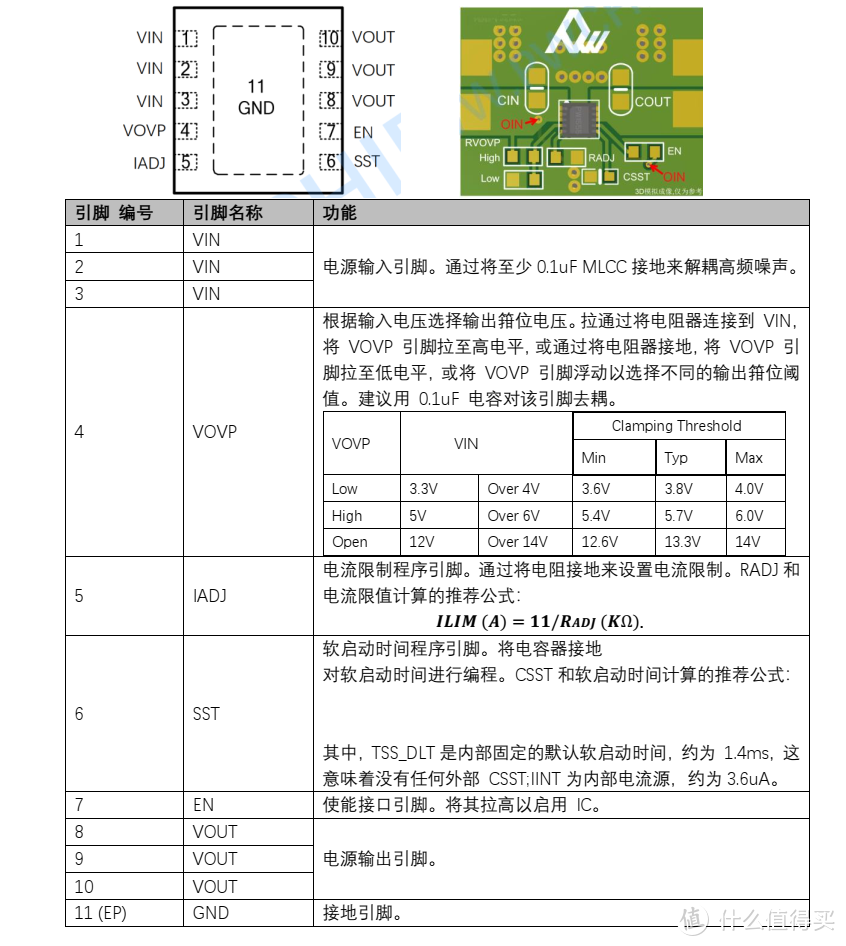
引脚分配/说明
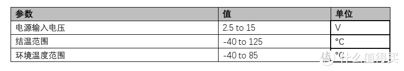
推荐操作条件 (note3)
Note 1: Stresses beyond “Absolute Maximum Ratings” may cause permanent damage to the device. These are for stress ratings. Functional operation of the device at these or any other conditions beyond those indicated in the operational sections of the specifications is not implied. Exposure to absolute maximum rating conditions may affect device reliability.
Note 2: θJA is measured in the natural convection at TA = 25°C on a low effective single layer thermal conductivity test board of JEDEC 51-3 thermal measurement standard. Test condition: Device mounted on 2” x 2” FR-4 substrate PCB, 2oz copper, with minimum recommended pad on top layer and thermal vias to bottom layer ground plane.
Note 3: The device is not guaranteed to function outside its operating conditions
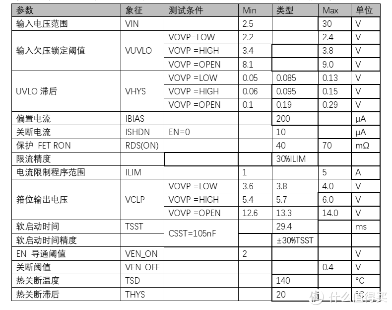
电气特性
(VIN = 5V, RADJ=10kΩ, CSST=105nF, CIN = 10uF, COUT = 10uF, TA = 25°C,除非另有说明)
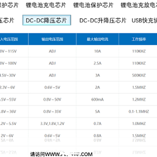
相关了解|DC-DC升压芯片代理|DC-DC降压芯片代理商|升降压芯片|锂电池充电芯片1节,两串,三串,四串等|LDO稳压芯片|MOS管|传感芯片等|夸克微科技